Beyond Precision, Beyond Future
Today, the Analog Components, on an average, contribute to 60%-70% of the real estate on the silicon. In order to spin these silicon out successfully, there needs to be a very strong Analog IP expertise, including the hardcore Analog circuit design expertise, Integration knowledge and Strong benchmarking capabilities. Now-a-days, these forces drive silicon based product solution companies towards having a top class in-house Analog, RF and MEMS team to ensure seamless and successful chip development cycle.
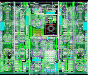
We, at BlackPepper, believe that Analog is the future of the silicon, also the solution to many problems of exponentially scaling up digital world, as seen today. So we have put in years of effort in building the strong Analog expertise internal to the company. With us, there is a mixed blend of Analog Circuit Design as well as Layout Design capabilities in the areas of IP design, Foundation IP, RF design etc. Another area of focus is the Transistor level design of analog and mixed-signal circuits for smart power stages and other low power management functions. The team has the experience of handling and owning the complete IP design from scratch in advanced technology nodes adhering to any of the design specification. The team has worked for customers in wireless, automotive, connectivity, consumer applications, medical and IoT markets.
We work with marketing, sales, application engineers and customers to help define new products and support our customers in the following areas
Analog IP Circuit Design and Layout
• PLL
• SERDES
• HDMI
• PCIe
• USB
• DAC
• ADC
• MIPI
• GPIOs
• Amplifiers
• Differential Clock Buffers
• Oscillators
• Bandgap References
• Thermal Sensors
• Low DropOut Regulators (LDO)
• Switched Capacitor Circuits
• Power Management Blocks
• Custom circuit and layout
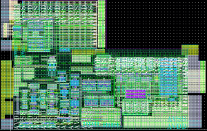
Foundation IP Design, Layout and Characterization
• Standard cells
• Memory compilers
• I/O cells
Analog Test Chip support
Analog verification support
Full chip signoff support (LVS, DRC, EM, ESD, Antenna, DFM)
Technology experience on varying process nodes from 130nm to 7nm
Proficiency in working with tools from Cadence, Synopsys, Intel, Mentor
SERDES, DAC, ADC
- Technology : 10nm, 14nm, 16nm, 28nm
- Process : GF, TSMC, SMIC
- Complete ownership of layout for SERDES, DAC, ADC starting from scratch
- There were different challenges meeting the specification and parasitics during the project execution. More challenges on EM & IR fixes.
- Timely completion and delivery of the assigned blocks across several technology nodes.
- Analog Blocks for SERDES: Phase interpolator, PGA, cap filter, bias blocks etc.
- Analog Blocks for DAC/ ADC: DAC,R2R ladder, bias blocks etc.
- Tools: Customer internal tool for Layout and Calibre, PVS for Verification
- PLL
- Technology : 28nm,65nm
- Process : TSMC, Fujitsu
- Complete ownership of PLL layout.
- Main constraints were delay matching of VCO block and parasitic coupling of high frequency clock lines.
- Done the top level floor planning , signal routing , power routing and post layout modifications of Digital PLL(DPLL).
- Used various layout techniques like matching , shielding to reduce process variations and parasitic couplings.
- Have closely worked with the designer in EM-IR analysis and parasitic analysis and fixed the issues.
- On time delivery of the block in different technology nodes.
- Tools: Cadence Virtuoso for Layout and Calibre, PVS for Verification.
IO Cell-Layout
- Technology : 14nm,40nm, 65nm
- Process : Intel, TSMC, Fujitsu
- Worked on LVCMOS and General purpose IO-cells.
- Developed different signal and power IO layouts from scratch. Taken care special ESD requirements while doing the layout of ESD protection devices.
- Have closely worked with the designer and fixed the project specifications like EM, Density-issues, Latch-up and ESD.
- Done the area estimation and floor planning.
- Done the ring level DRC and density verifications.
- Tools : Cadence Virtuoso for Layout, Calibre, PVS, IC-Validator and Totem for Verifications.
Ultra High Performance Memory Compiler Layout
- Technology : 14nm
- Process : GF
- Row banking : Multi bank
- Power domains : Memory/Core
- Complete ownership of compiler instance development, leaf cell floor planning to power planning, top level integration and physical verification.
- There were different challenges during the project execution : Netlists and layout reuse. Most of the netlists had to be corrected during LVS run and this consumed more time in debugging. Control block from different compiler had to be integrated into this compiler to minimize the layout effort .
- Minimum area usage for periphery circuitry making the compiler area efficient.
- eAgleSIght™ Analog Circuit Design and Implementation Frame Work