 Leaving no node unturned
Maximum Coverage, Low DPPM, Minimum Cost and Improved Yield are the key performance indicators for any successful chip design company to master the art of DFT.
At Simask’s we have a highly skilled and experienced team rendering services both in Front End and Backend DFT. Our primary focus is to provide silicon with least defects and optimized test time which in turn reduce the cost. Our DFT methodology provides a complete solution including MBIST, regular scan, AC scan, scan compression, boundary scan (JTAG), power aware test and ATPG, to achieve limit tending to 100% test coverage. We have been supporting customers across the globe on the whole spectrum of DFT flow from test architecture definition all the way to silicon bring up.
As a unit we offer our services in the following key areas.
Design For Test
• Test Methodology and Flow Development
• Test Architecture Proposal, Review and Implementation
o Scan Compression techniques
o Scan, BIST, JTAG structure insertion
o Custom Test block design for SoC
o Special Test support for Analog HM
o Special test for complex IOs and IOs
• Interface to Test house during Specification
• ATPG Flow Development
• ATPG coverage analysis and enhancement
• Serial and parallel pattern simulations
• Fault grading for Optimal Test Vector set
• Power Aware Test Implementation
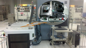
• Post-Silicon bring up support
New Product Introduction (NPI) Test Services
• Test Plan
• Test Specification
• Virtual Test Simulation at logic freeze, tapeout
• Tester H/W design ( Probe card, load board)
• Test Pattern Conversion and GLS/RTL simulation
• Test Program Development (for Wafer/Package)
• Test program development for Alpha, Beta Samples.
Product Qualification Test Services
• ATE Matrix lot product characterization
• Engineering data analysis
• Test Support for product qualification (ESD, Latchup, Burn-in, HTOL etc)
• Test Support for Device correlation/ reliability
• Test Support for tester H/W tester correlations
• Test support for device production release.
• Remote debug
Production Test Service
• Test time reduction
• Production and low yield lot analysis
• Yield enhancement
• CQI( Customer Quality Incident) analysis
Tester tools capability
• Teradyne J750, Integra Flex ,Ultraflex
• Verigy , Agilent Oscilloscope
• Thermal Stream
 DFT Implementation, Verification and post silicon bring-up of Test and Product chip release of a Gigabit Ethernet Chip for High Speed Robotic Application
- Scan with customized On-chip compression XOR logic for a block with wide-1 masking logic.
Test Coverage Improvement
- Customized JTAG (Boundary Scan) / Stuck-at / Transition fault delay / IDDQ pattern generation, optimization & verification
- Customized JTAG supports Standard, custom instructions. IDCODE supports configurable part number and version id numbers.
- Coverage requirement for Stuck-at fault test(98 %), Transition delay fault test (85 %) and IDDQ test (20 measurement points)
- Technology: 40nm
- DFT Architecture: Flat DFT (Customized JTAG and Compression)
- Gate Count: 0.8M
- Clock Domain: 8
- Max Frequency: 125MHz
- Stuck-at TC: 98%
- Vector Count: 0.075M
- MaxDFX ™ One saop solution frame work for all DFx activities