First Pass Silcon Realizatiion Experience, Everytime
Physical Implementation business unit within Simask’s is one of the seasoned groups within the company, housing a highly experienced world-class team that has churned out multiple first pass silicon’s in advanced technology nodes for varied class of customers across wireless, automotive, connectivity, consumer applications, medical, IoT markets. This team has the experience of taking a design from early premature RTL stage to supplying end silicon’s volumes to customers.
They have engaged with customers early-on in their design flow and enabled them to define/improvise their designs, flow there-in reducing their design/implementation cycle time. This innovative thought process and engagement style has provided a huge monetary benefit for the customer and business continuity, fresh opportunities for Simask.
The team has worked on cutting edge technologies, designs and have been innovative in their offerings for each and every customer. The group has been constantly upgrading their knowledge base and can support customers in the following areas
- Experience of handling silicon’s in Wireless, Automotive, Connectivity, Consumer Applications, Medical, IoT domains.
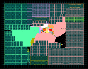
- Hierarchical Full Chip SoC Implementation.
- Hierarchical IP/Subsystem Implementation.
- High Speed IP/Subsystem Implementation (ARM, GPU, DSP, WLAN IP subsystems).
- Complex Block Implementation (Modem, Camera).
- Physical aware Synthesis for Full Chip, Block.
- Full chip, Block level signoff closure (static timing analysis, formal verification, dynamic and leakage power, physical verification, low power).
- Advanced low power design Implementation (DVFS, Switch Cells, MTCMOS).
- Flow and methodology support.
- Technology experience on varying process nodes optimized for performance, power ranging from 28nm, 20nm, 16nm, 10nm, 7nm.

Delivered a dual ARM based mobility SoC for a key customer in the wireless space in a record time of 5 weeks from the final netlist to tape-out.
- Die Size 57.96 sq mm , TSMC 45nm with LVT, 6LM [5 thin, 1 thick (4x)] + 1 AP RDL layer
- ARM Quad Core (A5) @ 1.2 GHz, DDR2, 4 MIPI, Graphics Core
- 5.6M instances, RAM – 31.75 Mbits, ROM- 1.2866 Mbits
- Package 11×11 mm, 576NSP
Delivered an accelerator soc for a tier3 customer from RTL to engineering samples in a short span of 5 months.
- Die Size 10 sq mm , TSMC 28nm HPC+, 9LM [6 thin, 2 thick (4x)] + 1 AP RDL layer
- 120 pin QFN package with paddle
- 4 Multifunction accelerator cores running @ 600 MHz
- 1.2M instances, Memory size – 1MB
Delivered a modem LTE subsystem from netlist to gdsii for a tier1 wireless customer. This was executed with a lean team with a very reduced time line in comparison with it’s earlier version.
- 13.6M Instances, 19.5 sq mm, , TSMC 16nm, 36 Blocks, 6 superblocks, Hierarchical Block with 3 Level deep hierarchy
Delivered 4 high speed DSP cores for a tier1 customer in the mobility market.
- 6.124 sq mm area, Samsung 14lpp, 10M_3Mx_4Cx_2Kx_1Gx + 1 RDL
- DSP cores delivering the modem functionality (Vector, Scalar Processing )
- 3.5M Instances, 500 Macros running at Fmax of 850 MHz
- 4 power domains with all advanced low power concepts (Switch cells, Isolation, Level Shifters)
Delivered the first ARM octa core cluster from netlist to gdsii for a wireless major in a short execution window of 3 months
- 64Bit ARMv8 architecture compliant “OCTA CPU” cluster
- CPU Cluster configuration
- o 4xA57 @ 1.8Ghz 2MB L2, 48KB L1I, 32 KB L1D
- o 4xA53 @ 1.4GHz 512KBL2, 32KBL1 I & D
- o coherently connected through CCI-400 @ 800Mhz interconnect
- 23.47 sq mm area, TSMC 28nm, 11 LM (9 + 2 RDL)
- 13 M Instances implemented as 6 Hierarchical Blocks
Delivered an IoT based Health sensing device for a Fabless Semiconductor Company from RTL to GDSII
- First single chip wireless health monitoring device
- Integrated with Dual ARM Cortex M0 cores
- Embeds three ultra-low-power radios for Wi-Fi, Ultra-wideband, and Medical Band (MBAN),
- Complete ownership of the chip from RTL2GDSII including all the signoff checks
- 14.96 sqmm, TSMC 90nm , 7 LM, 352kB RAM
Delivered a connectivity soc for a tier2 customer from netlist to GDSII
- Operating frequency 1GHz
- SOC implemented as 2 DIE’s
- 1 DIE ~200sqmm TSMC 7nm 15+RDL LM
- 1 DIE includes 15 blocks, 4 implemented as hierarchical blocks, different blocks instantiated multiple times
- ~30M*4 instances flat DIE, average instance per block >1M